1. Product Characteristics
Thin film circuits are made of high performance inductors, resistors and conductor lines fabricated by delicate photo-masking and thin film processing on substrates of isolated materials, deposited with several different thin film metals. A high performance and reliability hybrid microwave integrated circuits (HMIC) can be formed by die-attaching active devices and other required components on this substrate with thin film circuits. The advantages of a HMIC circuit are small size, light weight, good heat dissipation, high frequency, wide bandwidth, and high reliability. It typically operates from 1 to 20 GHz and even up to millimeter wave. They are very suitable for applications in defense radar, communication, electronic counter measure, and guidance systems, as well as commercial wireless communication equipments.
2��Substrate Types and Material Specifications
A. Substrate Material Specifications
|
Properties |
Polished Alumina
��Al2O3�� |
Asfired Alumina
��Al2O3�� |
Beryllium
Oxide
��BeO��
|
Aluminum Nitride
��AlN�� |
Fused Silica
��SiO2�� |
|
Chemical Composition |
Al2O3 |
Al2O3 |
BeO |
AlN |
SiO2 |
|
Purity (%) |
99.6 |
99.6 |
99.5 |
98 |
100 |
|
Density (g/cm3) |
3.87 |
3.87 |
2.85 |
3.28 |
2.2 |
|
Coefficient of Thermal Expansion (CTE) (ppm/��)
|
7.0-8.3
(25-1000��) |
7.0-8.3
(25-1000��) |
9.0 (25-1000��) |
4.6
(25-300��) |
0.65
(25-320��) |
|
Conductivity (W/m��K)
|
26.9 |
26.9 |
270 |
170 |
1 |
|
Dielectric Constant (��r) |
9.9
@25��1MHz |
9.9
@25��1MHz |
6.5
@25��1MHz |
8.6
@25��1MHz |
3.8
@25��1MHz |
|
Dissipation Factor (Loss Tangent) ( @ 1MHz) |
0.0001 |
0.0001 |
0.0004 |
0.001 |
0.000015 |
|
Isolation (kV/cm) |
4000 |
4000 |
--- |
--- |
10000 |
|
Grain Size (��m) |
<1.0 |
<1.0 |
9 �C16 |
5 �C 7 |
Amorphous |
|
Hardness (Rockwell) |
87 |
87 |
45 |
n/a |
7Mohs |
|
Flexural strength
(K(10-3) lbs/in2) |
90 |
90 |
35
(3pt.bend) |
59
(4pt.bend) |
25 |
|
Compressive strength
M(10-3) lbs/in2 |
54 |
54 |
---- |
---- |
161 |
|
Substrate size ��inches) |
1-3 |
1-3 |
1-2.25 |
1-2.25 |
1-2.25 |
B. Substrate size:
1���1�� (25.4 mm��25.4mm)
2.0���2.0�� (50.8 mm��50.8mm)
2.25���2.25�� (57.15 mm��57.15mm)
3.0���3.0�� (76.2 mm��76.2mm)
C. Substrate thickness:
0.005�填0.025�� (0.127mm��0.635mm)
0.005�塢0.010�塢0.015�塢0.02�塢0.025��, standard thickness ,
For other substrate thickness, please contact our sales department.
D. Substrate degree of finish: <4��-inches (0.1��m)
3. Standard Metalizations
TiW = 300�C800Å (0.03�C0.08µm)
Au = 20�C500µ" (0.5µm�C12.7µm)
TaN = 10�C200 ohms/square are available.
50�C75�C100 ohms/square are standard.
Typical TCR = �� 50ppm/��C
For other thin film metals, please contact our engineering department.
4. Standard Dimensions and Tolerances
Minimum line-width:
Typical 0.0004" (10.2µm) (plate-up process);
Typical 0.0008�� (20.4 um) ��etch-back process��
Smaller dimensions may be available.
Minimum Gap:
Typical 0.0004" (10.2µm) (plate-up process)
Typical 0.0008�� (20.4 um)��etch-back process��
Smaller dimensions may be available.
Resistor Minimum Length and Width:
Typical 0.002" (50.8um)
Smaller dimensions may be available.
Dimensional tolerance on critical areas:
Typical �� 0.0001" (2.5µm)
Dimensional tolerance on non-critical areas:
Typical �� 0.0003" (7.6µm)
Circuit Dimensional tolerance:
Typical �� 0.002" (50.8µm)
Resistor tolerance:
Typical �� 10%
5��Thin Film Circuits Design Rules
1.0 PURPOSE
1.1 This document defines the design rules for the thin film circuits and applies to all thin film circuits manufactured by Fidelics.
1.2 This document is divided into three sections:
1. Fundamental design rules.
2. Mask (tooling) requirements.
3. The resistor design rules.
2.0 FUNDAMENTAL DESIGN RULES
2.1 Substrate material type, thickness and surface finish must be specified.
2.2 Requirements for substrate surface metalization must be specified. These include metal types, thickness
and tolerances for both sides of the substrate. Our typical Au thickness on the substrate front side is
135~160 microinches (3.4~4.0 microns). Our typical Au thickness on the substrate back side is
40 microinches (1 microns).
2.3 Our standard processing requires circuits to be in square or rectangular.
2.4 All circuits must only feature straight lines, arcs, or their combinations. Irregular curves are not
acceptable.
2.5 Etch back process: minimum nominal conductor line width is 0.0004" (about 10 microns) if the gold thickness is 160 microinches (about 4 microns) or less. Plate up process : minimum nominal conductor line width is 0.0008" (about 20 microns) if the gold thickness is 160 microinches (about 4 microns) or less.
2.6 Etch back process: minimum nominal conductor gap width is 0.0008" (about 20 microns) if the gold thickness is 160microinches (about 4 microns) or less. A 0.0006�� (about 15 microns) gap is also achievable. Plate up process :the line width can be the smallest gap 0.0004 " (about10 microns), this applies to the thickness is 160microinches (about 4 microns) or less.
2.7 Critical dimensions have a standard minimum nominal tolerance of ��0.0001" (��2.5 microns) if the gold
thickness is 160 microinches (about 4 microns) or less. Tolerance on non-critical areas is �� 0.0003" (��7.6 microns).
2.8 The standard tolerance for Au thickness is ��20%.
2.9 Minimum nominal resistor width or length is 0.002" (50.8microns).
2.10 The tantalum nitride resistor has a stabilized sheet resistance of 50 ohms per square. Other values may
be available if required. Standard resistor tolerance is ��10%.
2.11 All circuits containing thin film resistors should have an isolated 50 ohm test resistor. This is especially
important for circuit designs with non-measurable resistors.
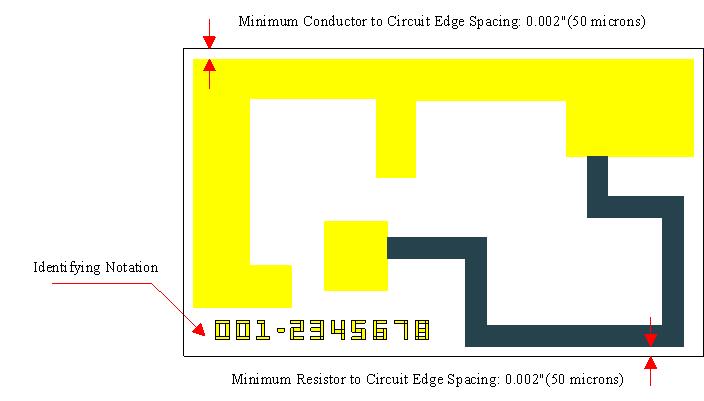
2.12 All conductors and resistors should be a minimum of 0.002" (about 50 microns) from the edge of the circuit ( figure 1).
figure 1
2.13All circuits should have an identifying notation of the conductor layer. ( figure 1)
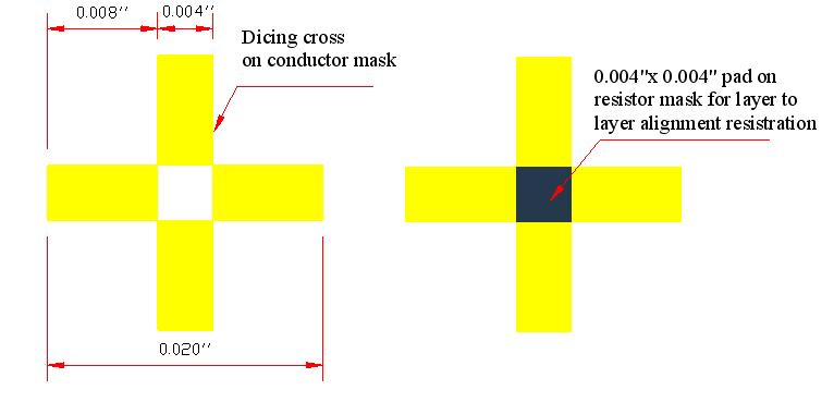
2.14 The dicing mark should be located on the conductor layer. The preferred dicing mark is a
0.004��x0.020�� (101x508 microns) cross as shown in the figure 2.
2.15 A 0.004��x0.004�� (0.1mmx0.1mm) pad on the resistor mask is used for layer to layer alignment
registration as shown in the figure 2.
2.16 Other dicing marks and alignment marks can also be used. However, they should be pre-approved by Fidelics.
figure 2
2.17 The standard dicing tolerance (for a final circuit size) is ��0.002" (�� 50 microns).
3.0 MASK (TOOLING) REQUIREMENTS
3.1 Conductor Mask��ETCH-BACK PROCESS��
3.1.1 The conductor geometry is dark and the field is light (positive photo-resist used).
3.1.2 With the emulsion/chrome side down, the conductor pattern and the part number should be right
reading.
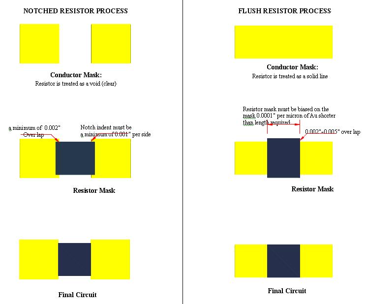
3.1.3 For a notched (island design) resistor design, a resistor-to-be area is treated as a void (clear) (figure3).
3.1.4 For a flush resistor design, a resistor-to-be area is treated as a solid block ( figure 4).
3.1.5 An etch factor must be built in all critical dimensions for the etch-back process.
Gaps must be biased on the mask with 0.0001" (2.5 microns) per 40 microinches (1 micron) of Au on the substrate, narrower than the nominal dimension ��e.g. If the Au thickness is 160 microinches (4 microns). a gap bias of 0.0004" (10 microns) narrower should be applied.��.
Line widths must be biased on the mask with 0.0001" (2.5 microns) per 40 microinches (1 micron) of Au on the substrate, wider than the nominal dimension. (The etch factor is required due to the undercutting of the Au layer by the etchant during the conductor patterning process).
3.2 Conductor Mask (plate up process)
3.2.1. The conductor geometry is light and field is dark(positive photo-resist used).
3.2.2. The conductor pattern and the part number are right reading with the emulsion/chrome side down.
3.2.3. A notched(island method) resistor is treated as a void(clear)(see figure 3).
3.2.4. All critical dimensions for the plate up process must have an exposure factor built in .Gaps must be biased on the mask with 0.00016" (4 microns) wider than the nominal dimension .Line widths must be biased on the mask with 0.00016" (4 microns) narrower than the nominal dimension.(The exposure factor is required due to the combination of light diffraction during exposure and the use of a thick photoresist >5 micron).
3.3 Resistor Mask For A Notched Resistor Design (Etch-Back Process)
(Fidelics Recommended Design)
3.3.1 The resistor geometry is dark and the field is light (positive photo-resist used).
3.3.2 The resistor pattern and the part number are right reading with the emulsion/chrome side down.
3.3.3 The notch indent for all notched resistors ( figure 3) must be a minimum of 0.001" on both sides.
Resistor edges should not be flush with the conductor geometry.
3.3.4 Resistors must have a minimum of 0.002" (50 micron) overlap onto the conductor line. Etch and/or
exposure factors are not required with the notched resistor process ( figure 3).
3.4 Resistor Mask For A FLUSH RESISTOR PROCESS (Etch-Back Process)
3.4.1 The resistor geometry is light and the field is dark (positive photo-resist used).
3.4.2 The resistor pattern and the part reading are right reading with the emulsion/chrome side down.
3.4.3 Resistor geometry must have a minimum of 0.002" (50 microns) to a maximum of 0.005" (127
microns) overlap wider than the conductor line. Resistor lengths must be biased on the mask 0.0001"
(2.5 microns) per 40 microinches (1 micron) of Au on the substrate, shorter than the nominal length of
the resistor ��e.g. If the Au thickness is 160 microinches (4 microns), the resistor length bias of 0.0004"
(10 microns) shorter should be applied.�� (figure 4).
figure 3 figure 4
3.5 CIRCUIT ARRAY
3.5.1 The mask array directly determines what kind of the substrate size can be used. The size of the substrate used to fabricate your parts heavily influences the final cost of the circuit. The array size required depends on the circuit size and the quantity ordered�� If you are providing the masks, please contact us to determine the optimum array size. Standard array sizes are 2"x2", 2.25"x2.25"��and 3"x3".
3.5.2 The standard border distance between the edge of the array and the edge of the substrate is 0.050"
(1270 microns).
3.5.3 The standard dicing kerfs (saw street width) is 0.007" (180microns).Other size can be accommodated. Please contact us for additional information.
3.5.4 The stepping distance of the circuits in the array is determined by adding the dicing kerf to the
circuit size. The dicing alignment mark (section 2.14) must be centered at each intersection.
3.6 SUBSTRATE MATERIALS
The following is a list of the standard materials processed
|
|
Alumina (Al203)Asfired surface finish
��Al2O3�� |
Alumina (Al203)Polished surface finish
��Al2O3�� |
|
MATERIAL THICKNESS |
0.005" |
0.005" |
|
0.010" |
0.010" |
|
0.015" |
0.015" |
|
0.020" |
0.020" |
|
0.025" |
0.025" |
Other materials are also available. These include: Beryllium Oxide, Aluminum Nitride, Quartz/Fused Silica.
4.0 The Resistor Design Rules
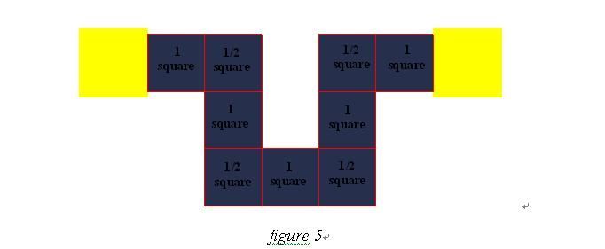
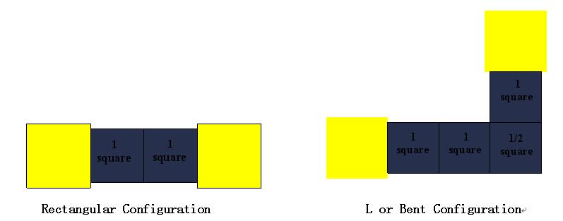
4.1The resistance of a specific resistor is determined by the ratio of its length to width, which is expressed as a number of ��squares�� .
4.2 The equation for calculating resistance is: R = s(L/W)
R = resistance in ohms
s = sheet resistance in ohms/square
L = length of the resistor
W = width of the resistor
4.3 Resistor ��length�� is always the dimension of the resistor parallel to the current flow.
4.4 The resistor ��square�� in the corner area(s) of a bent style resistor (e.g. an ��L�� shape or serpentine design)
should be counted as one-half the value of the sheet resistance. ( figure 5)
4.5 RESISTOR TYPES
4.5.1Rectangular Configuration: The most common type of resistor. (See figure 6)
Rectangular Configuration L or Bent Configuration
figure 6 figure 7
4.5.2 L or Bent Configuration: The resistor ��square�� in the corner area of a bent style resistor should be
counted as one-half the value of the sheet resistance. (figure 7)
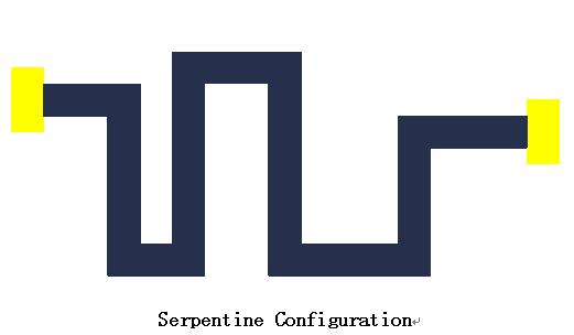
4.5.3 Serpentine Configuration: This resistor is typically used for high value resistors. The number of
corners complicates calculation of the value. The resistor ��square�� in the corner areas of a serpentine
style resistor should be counted as one-half the value of the sheet resistance. ( figure 8)
Serpentine Configuration
figure 8 |